Series Resonance is a phenomenon at which the net reactance of the circuit is zero or inductive reactance is equal to capacitive reactance.
Circuit Diagram & Derivation of Series Resonance
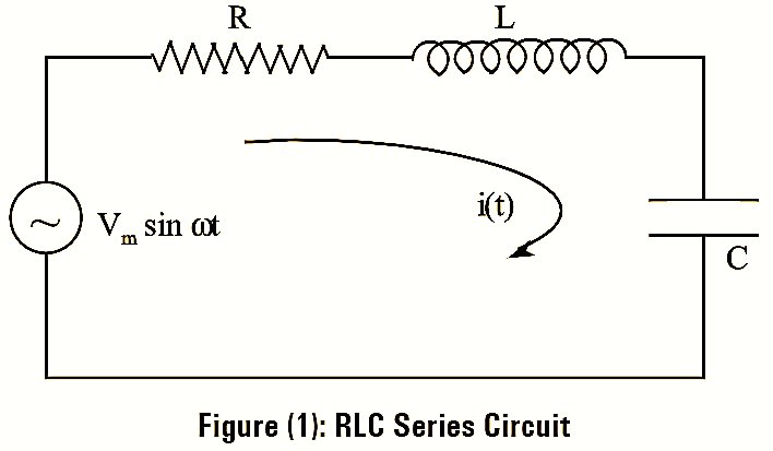
Let, V = Vm sin ωt be the voltage applied across it and i(t) be the current flowing through it. In case of series RLC circuit, the net impedance is given by,
\[Z=R+j\left( {{X}_{L}}-{{X}_{C}} \right)\]
Where,
XL = Inductive reactance
XC = Capacitive reactance.
From equation (1) it is clear that there exist three effects in the circuit i.e., the resistive, inductive and capacitive effect.
However, the effect of resistance is inherent hence a series RLC circuit either behaves as inductive or capacitive depending on the relative value of XL and XC If XL > XC the circuit behaves as inductive circuit and if XC > XL the circuit behaves as capacitive circuit. However, if these two values are equal i.e., XL = XC the net reactance will be zero and the circuit is said to be under resonance.
Expression for Resonant Frequency of Series Resonance
The frequency at which resonance occurs is called as resonant frequency. The condition for resonance is,
XL = XC
But, we know that,
\[{{X}_{L}}=2\pi {{f}_{r}}L\]
\[{{X}_{C}}=\frac{1}{2\pi {{f}_{r}}C}\]
Where, fr is the resonant frequency in Hz.
Substituting the above values in equation (2), we get,
\[2\pi {{f}_{r}}L=\frac{1}{2\pi {{f}_{r}}L}\]
\[f_{r}^{2}=\frac{1}{4{{\pi }^{2}}LC}\]
\[{{f}^{2}}=\frac{1}{4\pi \sqrt{LC}}\]
\[2\pi f=\frac{1}{\sqrt{LC}}\]
\[{{\omega }_{r}}=\frac{1}{\sqrt{LC}}\]
Where, ωr is the resonant frequency in rad/sec
Resonance Curves for a series resonant circuit with variable frequency and constant R, L and C
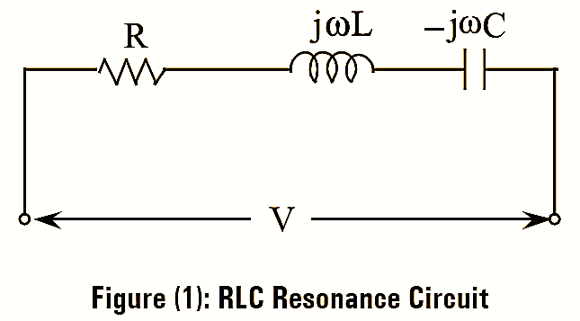
Figure (1) shows the circuit diagram of series RLC circuit, which has a complex impedance, Z = R +jX.
Where,
\[X=j\left( \omega L-\frac{1}{\omega C} \right)\]
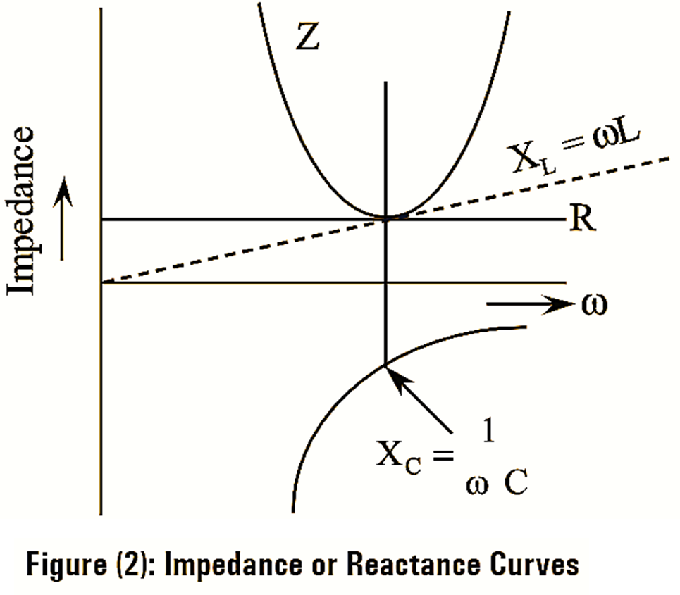
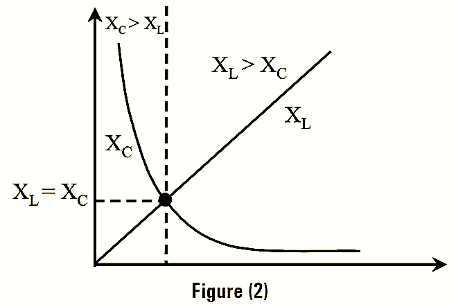
Figure (2) shows the variation of resistance, inductive reactance (XL) and capacitive reactance (XC) with frequency.
For Resistance
R is independent of frequency; hence it is represented by a straight horizontal line.
Moreover, at resonance XC = XL i.e., |Z| = R.
Hence, at resonance |Z| = R and thus at resonance the impedance (Z) is minimum.
For Inductance
\[{{X}_{L}}=\omega L=2\pi fL\]
It is a function of frequency i.e., inductive reactance is directly proportional to frequency (f), hence, its graph is a straight line through the origin as shown in figure (2).
For Capacitance
\[{{X}_{C}}=\frac{1}{\omega C}=\frac{1}{2\pi fC}\]
Capacitive reactance is inversely proportional to frequency (f). Its graph is a rectangular hyperbola as drawn in fourth quadrant, since, Xc is regarded as negative.
Total impedance,
\[Z=\sqrt{{{R}^{2}}+{{\left( {{X}_{L}}-{{X}_{c}} \right)}^{2}}}=\sqrt{{{R}^{2}}+{{X}^{2}}}\]
At low frequencies Z is large, the net impedance is capacitive and the power factor is leading (XC > XL) At high frequencies Z is again large but it is inductive (XL > XC) and the power factor is lagging.
Current (I)
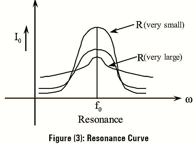
It has a low value of current on both sides of resonant frequency as Z is large but has the maximum value of current, \(\frac{V}{R}=I\) at resonance as Z is small, which is shown in figure (3). Hence, at resonance maximum power is dissipated by the circuit. The shape of resonance curve for various values of ‘R’ is also shown in figure (3). It is observed that, if R is large then current is less and vice-versa.
Phase Angle
At f = 0, XL = 0 by, 0 and XC = ∞ then the phase angle is given by.
\[\theta ={{\tan }^{-1}}\left( \frac{{{X}_{L}}-{{X}_{C}}}{R} \right)\]
\[={{\tan }^{-1}}\left( \frac{0-\infty }{R} \right)={{\tan }^{-1}}\left( -\infty \right)=-90{}^\circ \]
As the frequency is increased from zero, XL increases, XC decreases and hence phase angle moves from -90º and goes towards zero.
At f = fr, XL = XC and the phase angle is given by,
\[\theta ={{\tan }^{-1}}\left( \frac{0}{R} \right)=0{}^\circ \]
As the frequency is further increased beyond fr, the phase angle increases from 0º towards +90º.
At f = ∞, XL = ∞, XC = 0, the phase angle is now given as,
\[\theta ={{\tan }^{-1}}\left( \frac{\infty -0}{R} \right)=90{}^\circ \]
Hence the above points can be summarized as,
- At f = 0, XC = ∞, θ = -90º thus the current leads the voltage by 90º.
- At f < fr, -90º < θ < 0, the current leads the voltage by an angle θ.
- At f = fr, XL = XC, θ = 0º and the current is in phase with voltage.
- At f > fr , 0º < θ < 90º and the current lags the voltage by an angle θ.
- At f = ∞, XL = ∞, θ = 90º and the current lags the voltage by 90º.
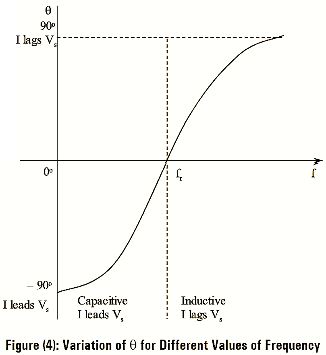
Figure (4) shows the variation of θ for different values of frequency.