Semiconductor Strain Gauge is also called piezo-resistive strain gauges. These are made up of doped silicon and germanium which have crystalline structure. When subjected to strain, resistivity of this material changes. This property is called piezo-resistive property.
(i)
(ii)
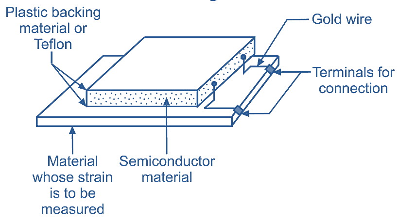
Fig. 1: Semiconductor Strain Gauges.
Construction & Working of Semiconductor Strain Gauge
Semiconductor gauges are manufactured in the form of filaments of rectangular cross-section (0.7 mm to 5 mm in length and width is 1/10th of length and thickness is about 0.05 mm). They are sandwiched between a plastic backing material or Teflon. The connections are brought through gold wire (Refer Fig. 1).
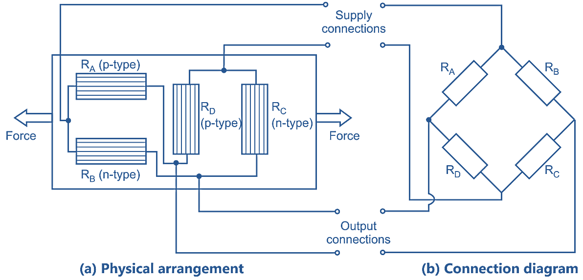
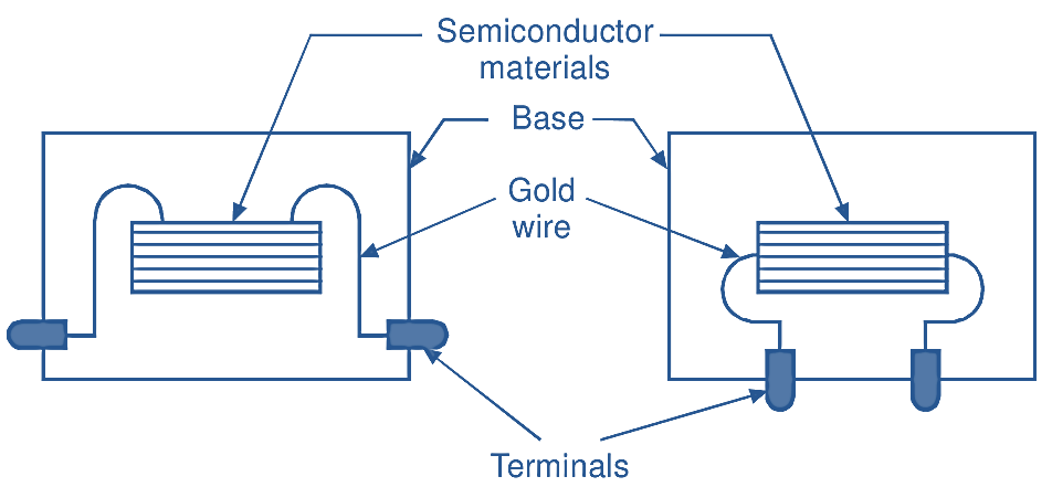
Fig. 2: Semiconductor Strain Gauge Physical arrangement and Connection diagram.
These silicon and germanium semiconductor strain gauges are doped with boron. Lightly doped gauges have gauge factors of 200 to 300 with electrical resistance of about 200 to 1000 Ω. Heavily doped semiconductor strain gauges have gauge factor of 50 with lower electrical resistance. These can operate in the temperature range of – 200 to 400°C. The semiconductor strain gauge can be connected in bridge form for strain measurement. (Refer Fig. 2).
By adjusting doping, p and n type of semiconductor, strain gauges are formed (RA, RB, RC, RD) and these are connected together to form a bridge circuit. When force acts on the material, strain is produced causing imbalance in the bridge and output voltage is obtained.
Advantages of Semiconductor Strain Gauge
- These possess high sensitivity or high gauge factor as compared to foil gauges. So generally these do not require any amplification in their output or alternatively these can be used with amplification for measuring very small values of strain.
- These are very small in size, hence they can be used for measurement of local strains or in places inaccessible to foil or wire gauges.
- Hysteresis characteristics are excellent.
- Life is more.
- They have got better frequency response.
Disadvantages of Semiconductor Strain Gauge
- These are very sensitive to temperature changes.
- Linearity is poor.
- More expensive.
Semiconductor Strain Gauge Circuits
There are two types of strain gauge circuits:
- Potentiometer circuit or voltage divider circuit.
- Bridge circuit.
Potentiometer circuit or Voltage divider circuit
The potentiometer circuit is shown in Fig. 3.
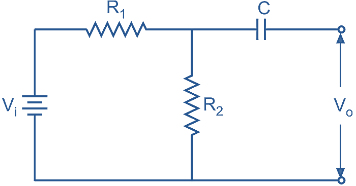
Fig. 3: Strain gauge potentiometer circuit
The strain gauge potentiometer circuit is shown above. Due to strain, R1, R2 change and this causes change in output voltage V0.
\[{{V}_{0}}=\left( \frac{{{V}_{i}}}{{{R}_{1}}+{{R}_{2}}} \right){{R}_{2}}\]
This is used for dynamic strain measurement.
Wheatstone’s Bridge Configuration and Full Bridge Configurations
The strain gauge gives some output even if strain is zero. This is known as offset or null error (Refer Fig. 4). Using bridge circuit for strain gauge, this error can be eliminated. This arrangement also eliminates temperature error. This is used for static strain measurement. The strain gauges are connected in the form of Wheatstone’s bridge form.
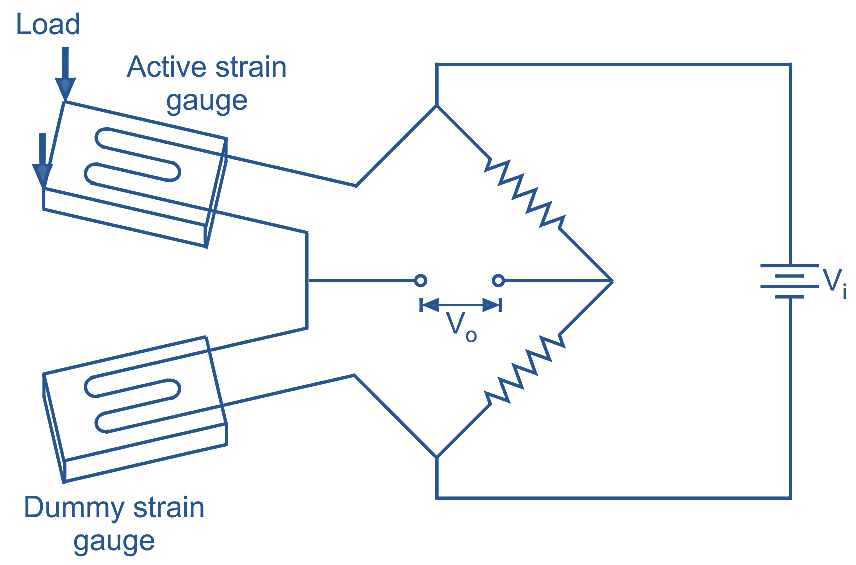
Fig. 4 : Wheatstone’s bridge connection for strain gauge